This article outlines how NVIDIA’s next-generation Blackwell architecture moves far beyond the H200, delivering a redesigned compute platform built for trillion-parameter models, real-time inference at massive throughput, and far greater energy and memory efficiency.
What you’ll learn:
- How Blackwell’s new compute core, expanded HBM, chiplet design and improved attention/mixed-precision operations differ from Hopper
- Expected capabilities of the B100, B200, B300 and Grace-Blackwell Superchip for large-scale training, fine-tuning and multimodal workloads
- Why chiplet-based scaling, higher memory bandwidth and optimized KV-cache handling redefine performance for long-context LLMs
- How next-gen NVLink and networking improve multi-node training efficiency and cluster scalability
- Practical performance expectations across training, fine-tuning and high-throughput inference
- Why Blackwell’s energy-efficiency and architectural integration will accelerate cloud adoption and reshape AI infrastructure planning
The H100 and H200 have defined the past two years of large-scale AI acceleration, powering frontier model training, high-throughput inference and the rapid rise of multimodal architectures.
But NVIDIA’s roadmap is already shifting again – and the next leap, the Blackwell generation, is not just an incremental gain over Hopper. It represents a redesigned compute platform built for trillion-parameter scale models, real-time inference at enormous throughput, and energy efficiency targets that match the realities of enterprise AI growth.
For CTOs, ML architects and infrastructure teams planning multi-year roadmaps, understanding what Blackwell brings – and how it differs from H200 – is crucial. This new generation is engineered to support the next wave of AI workloads: massive context windows, real-time agentic loops, multimodal reasoning and ultra-dense training clusters with far tighter interconnect integration.
Below is what teams should expect as the industry moves beyond the H200 era and into Blackwell-driven AI infrastructure.
The leap from Hopper to Blackwell
The move from H100 to H200 expanded memory bandwidth and boosted performance for transformer inference, but the architecture remained fundamentally Hopper. Blackwell, by contrast, introduces:
- a new compute core (Blackwell SM)
- dramatically expanded high-bandwidth memory
- architectural-level improvements to attention, sparsity and mixed-precision operations
- enhanced interconnect fabric for larger-scale multi-GPU clusters
- chiplet-based scaling that changes what “one GPU” even means
This jump mirrors the industry’s pivot from “just faster GPUs” to training and serving engines capable of sustaining multi-trillion FLOP workloads without thermals or networking becoming the bottleneck.
B100 and B200: the next compute workhorses
The first two major GPUs in the Blackwell line, the B100 and B200, are purpose-built for both giant LLMs and high-throughput inference.
Expected improvements include:
- Significantly higher tensor performance, particularly in FP8 and FP6
- Major gains in attention throughput, especially for long-context models
- Larger effective model capacity due to improved memory scaling
- Substantially better energy efficiency, delivering more performance per watt than H200
- Faster communication paths for distributed training
Teams should expect B100/B200 to outperform H200 by a large margin for both large-batch training and small-batch, low-latency inference – the two ends of the modern AI workload spectrum.
Where H100 was optimized primarily for training and H200 leaned toward inference throughput, Blackwell is designed to excel at both, simultaneously.
The Grace-Blackwell Superchip: a new class of AI compute
One of the biggest shifts isn’t just the GPU – it’s the GB200 Grace-Blackwell Superchip, which pairs Blackwell GPUs with NVIDIA’s Grace CPU.
This superchip effectively dissolves the traditional CPU–GPU boundary by providing:
- shared coherent memory
- massive bandwidth between CPU and GPU
- tight scheduling coordination for distributed workloads
- better performance on data-limited or I/O-heavy training
For pipelines with heavy preprocessing, reinforcement learning loops or multimodal fusion, the GB200 platform may offer large gains over Hopper-based architectures because it reduces CPU-side bottlenecks that often throttle GPU utilization.
Alongside the GB200 platform originally announced, NVIDIA has now expanded this line with the B300 GPU and the GB300 Superchip. These newer components build on the same design philosophy: higher memory capacity, improved interconnect throughput and significantly better performance per watt. The B300 serves as a next-step Blackwell GPU variant optimized for large-scale inference and fine-tuning, while the GB300 extends the CPU–GPU fusion model for even more demanding enterprise and hyperscale environments.
Cloud and enterprise providers are expected to adopt these chips quickly, not just for peak FLOPS, but for their ability to handle complex workflows that blend text, vision, audio and structured reasoning at unprecedented scale.
A chiplet design built for extreme scale
Blackwell is the first NVIDIA architecture built around a chiplet model, combining multiple dies into a single GPU package. This unlocks:
- much larger compute density
- higher memory capacity within the same thermal envelope
- lower latency between internal compute units
- better scaling of SM count without losing frequency or efficiency
Chiplets also improve manufacturing yields, which will matter as demand for compute continues to rise faster than fabrication capacity.
For infrastructure teams, the chiplet leap means that Blackwell GPUs will effectively behave more like miniature clusters – optimized for both intra-chip and inter-node parallelism.
Memory: the true bottleneck, redefined
Training and inference performance today is often limited by memory – not compute. Blackwell directly targets this choke point.
Expected upgrades include larger HBM stacks with higher capacities, increased aggregate memory bandwidth, more efficient partitioning for KV caches and intermediate tensors and potential architectural improvements such as on-chip memory compression.
These enhancements benefit a wide range of workloads, from LLM training with long context windows and multimodal models blending text, vision and audio, to high-throughput inference with substantial KV-cache demands and parallel model serving that relies on shared memory pools. Memory improvements alone may deliver double-digit percentage speedups beyond the raw FLOP gains.
Next-gen NVLink and networking for massive training clusters
One of the defining features of frontier-scale AI is the need for massive clusters with near-lossless communication. Blackwell’s updated NVLink, NVSwitch and networking ecosystem addresses this head-on.
Teams can expect:
- higher GPU-to-GPU bandwidth inside a node
- reduced latency for distributed attention
- better scaling across 16/32/64-GPU topologies
- stronger integration with next-gen InfiniBand and Ethernet fabrics
This matters because modern LLMs don’t scale linearly unless communication overhead stays close to negligible – especially during gradient synchronization or pipeline-parallel workloads.
Blackwell is designed to push cluster efficiency closer to theoretical maximums.
Performance expectations: training, fine-tuning, inference
While NVIDIA has shared the broad performance direction, here’s what engineering teams can expect in practical terms:
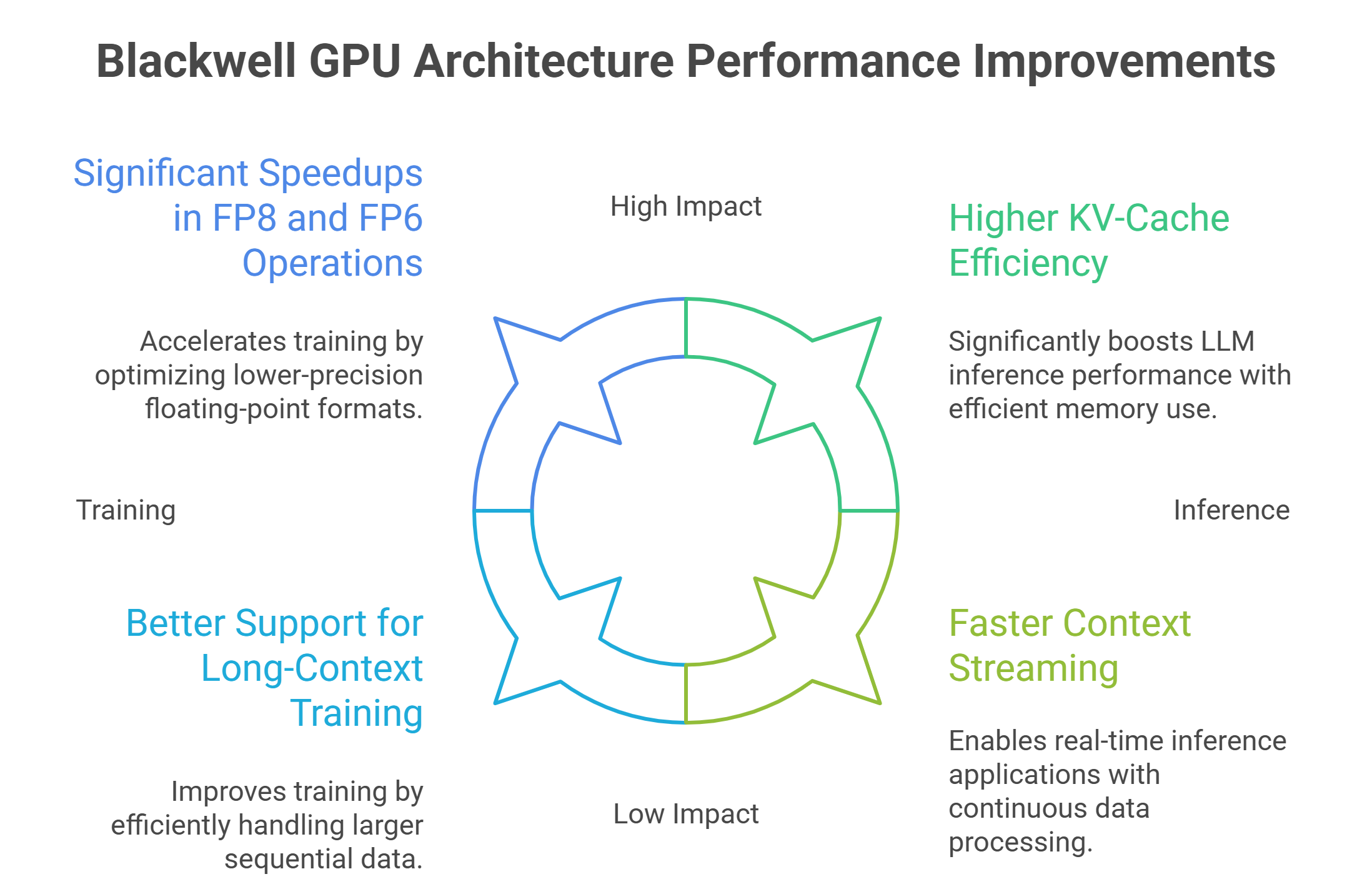
Training
- Significant speedups in FP8 FP6 operations
- Better support for long-context training
- Higher efficiency for dense and sparse transformer blocks
- Better scaling across multi-node clusters
Fine-tuning
- Lower memory pressure for parameter-efficient methods
- Faster quantization-aware pipelines
- Much better throughput for supervised fine-tuning and RLHF
Inference
- Higher KV-cache efficiency
- Faster context streaming
- Higher throughput per GPU for LLM inference
- Improved batching strategies via smarter memory access patterns
For teams building multi-model inference environments (RAG, embeddings, rerankers, agents), Blackwell’s efficiency improvements will likely translate into meaningful cost-per-token reductions.
Energy efficiency: a critical enterprise requirement
Compute demand continues to rise faster than power availability. Blackwell responds with architectural improvements that increase performance per watt, helping enterprises run larger clusters within the same power envelope, reduce cooling and datacenter overhead, and improve operational predictability as models scale.
This is especially important for hybrid deployments and operators optimizing for long-running training pipelines.
What this means for cloud adoption
Cloud adoption will accelerate around the Blackwell generation for several reasons:
- Demand for H100/H200 already exceeds supply; Blackwell will be even more sought after.
- Next-gen performance benefits disproportionately favor cloud-scale clusters.
- Chiplet designs and NVLink upgrades make multi-GPU nodes even more complex to operate on-prem.
- Enterprises will prefer managed infrastructures with tuned networking and scheduling.
For engineering teams building multi-year AI strategies, aligning with Blackwell-compatible infrastructure will matter.
The bottom line
NVIDIA’s Blackwell generation isn’t just the next step after H200 – it’s a redefinition of how AI compute scales. With chiplet-based design, higher memory bandwidth, faster interconnects, better energy efficiency and the Grace-Blackwell Superchip, it sets the stage for the next decade of AI infrastructure.
For CTOs, ML leads and infrastructure architects, the arrival of Blackwell marks a shift toward systems built not just for bigger models – but for continuous training, multi-model inference, agentic workloads and real-time applications that demand unprecedented throughput.
Frequently asked questions about NVIDIA Blackwell AI GPUs
1. How is NVIDIA Blackwell different from the current H200 generation?
Blackwell is not just a faster Hopper refresh like H200. It introduces a new Blackwell SM core, much larger and faster high bandwidth memory, architectural upgrades for attention, sparsity and mixed precision, stronger interconnect fabric and a chiplet based design aimed at trillion parameter scale models and ultra high throughput inference.
2. What roles do the B100, B200 and B300 GPUs play in AI workloads?
B100 and B200 are the main Blackwell GPUs designed to be the new workhorses for both giant LLM training and high throughput inference, with much higher tensor performance, attention throughput, model capacity and energy efficiency than H200. B300 builds on this as a next step variant optimized for large scale inference and fine tuning in demanding enterprise and hyperscale environments.
3. What is the Grace Blackwell Superchip and why does it matter?
The GB200 and GB300 Grace Blackwell Superchips tightly pair Blackwell GPUs with Grace CPUs, effectively dissolving the old CPU GPU boundary. They provide shared coherent memory, huge CPU GPU bandwidth and tighter scheduling, which helps in data limited, I O heavy, multimodal or reinforcement learning pipelines where CPU bottlenecks used to starve GPUs.
4. Why is the chiplet design in Blackwell important for scaling AI clusters?
Blackwell is NVIDIA’s first chiplet based GPU architecture, combining multiple dies into one package. This allows much higher compute density, more memory capacity in the same thermal envelope, lower latency between internal compute units and better scaling of SM count. In practice, each GPU behaves more like a tiny cluster tuned for both intra chip and inter node parallelism.
5. How does Blackwell improve memory and networking for large models?
Blackwell targets memory as a primary bottleneck with larger HBM stacks, higher aggregate bandwidth and more efficient handling of KV caches and intermediate tensors. At the same time, next gen NVLink, NVSwitch and networking bring higher GPU to GPU bandwidth, lower latency for distributed attention and better scaling across 16 32 64 GPU topologies, pushing cluster efficiency closer to theoretical limits.
Build AI Without Limits
GMI Cloud helps you architect, deploy, optimize, and scale your AI strategies
FAQ
Blackwell is not just a faster Hopper refresh like H200. It introduces a new Blackwell SM core, much larger and faster high bandwidth memory, architectural upgrades for attention, sparsity and mixed precision, stronger interconnect fabric and a chiplet based design aimed at trillion parameter scale models and ultra high throughput inference.